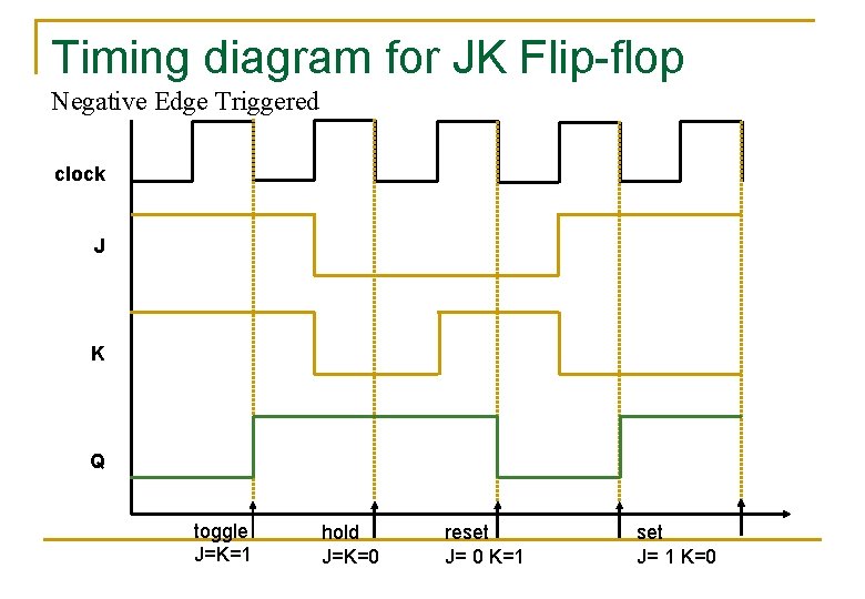
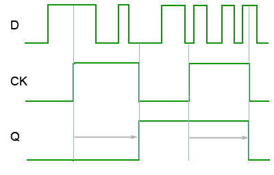
39 negative edge triggered jk flip flop timing diagram
April 20, 2021 - The TTL 74LS73 is a Dual JK flip-flop ... flop IC’s include the 74LS107 Dual JK flip-flop with clear, the 74LS109 Dual positive-edge triggered JK flip flop and the 74LS112 Dual negative-edge triggered flip-flop with both preset and clear inputs.... After every falling edge, when T = 1, the output state of Flip Flop will toggle. Initially Q 3 = 0 , Q 2 = 0 , Q 1 = 0.. Case 1 : When M=0 ,then M'= 1. T 3 = M'Q 2 Q 1 + MQ' 2 Q' 1 = Q 2 Q 1.; T 2 = M'Q 1 + MQ' 1 = 1.Q 1 = Q 1.; T 1 = 1.; Because T 1 = 1, therefore FF1 output state toggles for every falling edge. The output state of FF 2 will toggle when Q 1 = 1 and the falling ...
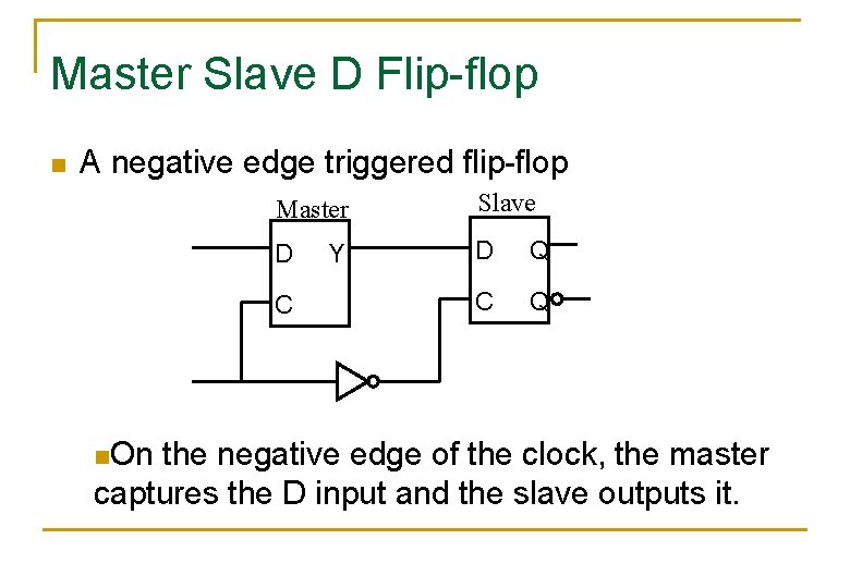
This circuit is a edge-triggered D flip-flop. It functions the same as a master-slave flip-flop (except that it is positive-edge triggered), but uses fewer gates in its design · The circuit consists of 3 set-reset latches. The latch on the right controls the output.
Negative edge triggered jk flip flop timing diagram
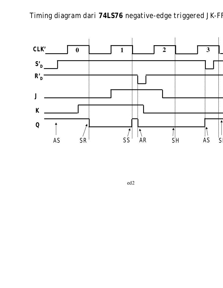
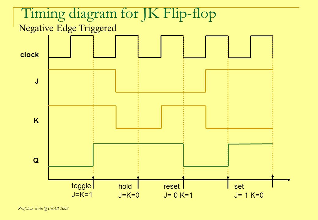
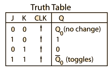
July 3, 2006 - The JK flip-flop is usually negative edge triggered. The truth table for a negatively triggered JK flip-flop: The timing diagram for the negatively triggered JK flip-flop: June 11, 2019 - A Counter is a device, which stores ... of times a particular event has occurred, often in relationship to a CLOCK Signal. In electronics, counters can be implemented quite easily using memory devices such as Flip-flops. J-K Flip-flop is one of the most commonly used Flip-flops. Table 1 is the Truth-Table of a Negative-Edge-Triggered J-K ... April 20, 2021 - Electronics Tutorial about the D-type Flip Flop also known as the Delay Flip flop, Data Latch or D-type Transparent Latch used in Sequential Circuits
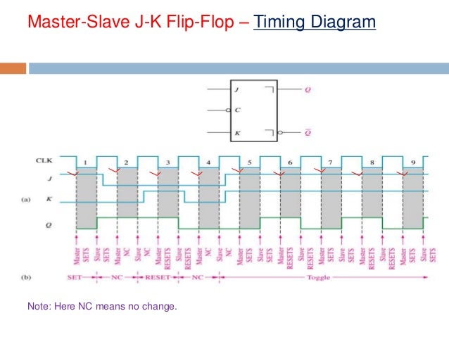
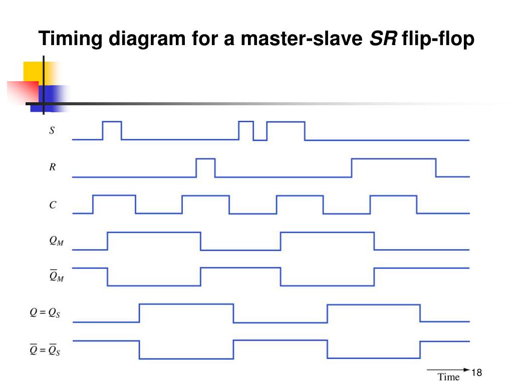
Negative edge triggered jk flip flop timing diagram. Flip-flops are synchronous bistable multivibrators with two stable outputs, one being the complementary state of the other. A Set-Reset (latch), Data (register), J-K, or Toggle flip-flop changes output state on the application of a clock or input edge-triggered command either with a positive rising-edge or negative falling-edge transition. Operation of a 2-bit synchronous binary counter using J-K flip-flop. The operation of a J-K flip-flop synchronous counter is as follows: First, assume that the counter is initially in the binary 0 state; that is, both flip-flops are RESET. When the positive edge of the first clock pulse is applied, FF0 will toggle and Q 0 will therefore go HIGH. AboutPressCopyrightContact usCreatorsAdvertiseDevelopersImpressumNetzDG TransparenzberichtNetzDG ComplaintsTermsPrivacyPolicy & SafetyHow YouTube worksTest new features · © 2021 Google LLC Master--Slave and Edge-Triggered J-K Flip-Flop
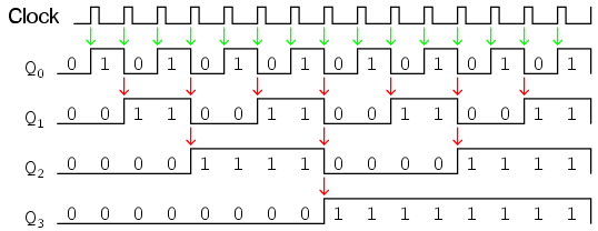
In this section, we will discuss the Logic diagram, Timing diagram, and operation of the Asynchronous Up counter for Negative edge-triggered flip-flops. Logic diagram. Figure (2.1) shows the logic diagram of the Asynchronous Up counter for negative edge-triggered flip-flops. In the figure below, you can see the arrangement of a clock signal for ... The below diagram shows the 3-bit asynchronous down counter. Since it is a 3-bit counter, 3 negative edge-triggered flip-flops are used. The clock pulse input is given only to the first flip-flop. The clock input of the remaining flip-flops is triggered by the Q output of the previous flip-flop. via YouTube Capture Therefore, Flip flop 3 output is toggle when there is clock falling edge and Q'2=1 and Q'1 = 1 .(as you can see from timing diagram) Therefore, we get output(as down counting Q3(MSB) Q2 Q1(LSB) after 8th -ve edge triggered clock the output of the three Flip flops again becomes Q3 = 0, Q2 = 0, Q1 =0.
Flip-flops, D-type flip-flops explained, Data latch, ripple-though, edge-triggering, synchronous and asynchronous operation. 9.4: Edge Triggered Flip-Flop. An edge triggered flip-flop (or just flip-flop in this text) is a modification to the latch which allows the state to only change during a small period of time when the clock pulse is changing from 0 to 1. It is said to trigger on the edge of the clock pulse, and thus is called an edge-triggered flip-flop. Your user agent does not support the HTML5 Video element · Illinois Tech stands at the crossroads of exploration and innovation, advancing Chicago and the world. Every day in the living lab of the city, Illinois Tech fuels breakthroughs that change lives In this lesson, we'll go over how to utilize latches to design a positive edge triggered flip flop
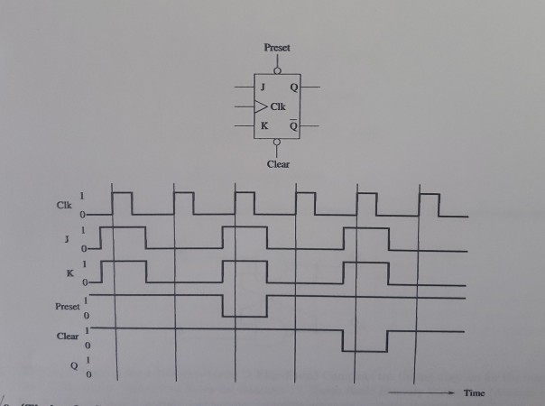
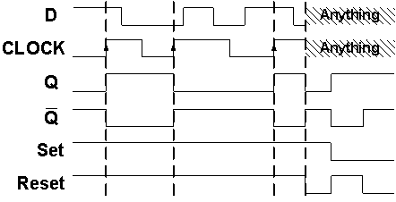
The operation and truth table for a negative edge-triggered flip-flop are the same as those for a positive except that the falling edge of the clock pulse is the triggering edge. As S = 1, R = 0. Flip-flop SETS on the rising clock edge. Note that the S and R inputs can be changed at any time when ...
In edge triggering, the flip flop changes its state during the positive edge or negative edge of the clock pulse. There are two types of edge triggering. Positive edge triggering - When the output responds to the change in the input only at the positive edge of the clock pulse, then the clock pulse is said to be a positive edge triggered.
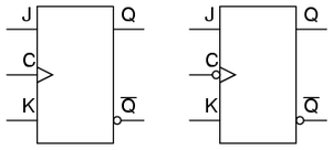
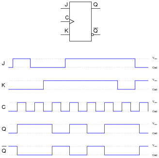
November 1, 2020 - In general it has one clock input pin (CLK), two data input pins (J and K), and two output pins (Q and Q̅) as shown in Figure 1. JK flip-flop can either be triggered upon the leading-edge of the clock or on its trailing edge and hence can either be positive- or negative- edge-triggered, ...

Welcome I would like to ask you for explain this timing diagrams. I got some assignments for reading timing diagrams and solved it but I am not sure if it is good. I have JK flip-flop which is pos...
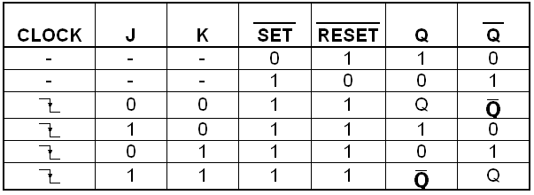
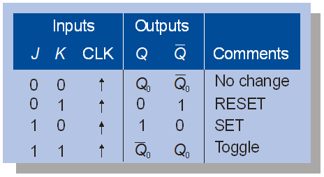
The J-K flip-flop block has three inputs, J, K, and CLK. On the negative (falling) edge of the clock signal (CLK), the J-K Flip-Flop block outputs Q and its complement, !Q, according to the following truth table. In this truth table, Qn-1 is the output at the previous time step.
Flip flops are actually an application of logic gates. A timing diagram illustrating the action of a positive edge triggered device is shown in fig. This circuit can be used to create a synchronized pulse based upon an asynchronous signal transition event.
A description of the JK and T flip flops along with some example timing diagrams showing how they work
March 18, 2021 - Read about Edge-triggered Latches: Flip-Flops (Multivibrators) in our free Electronics Textbook
Alexander Stoytchev Office: Howe Hall, Room 2624D Office hours: MWF after class 5:00-5:30pm in the classroom (Hoover Hall, Room 2055) (or by appointment) Phone: 515-294-5904 (email preferred) · Section N: Monday 9:00 AM - 11:50 AM (Coover Hall, room 1318) [Mohamed Selim, Gabriel Klein] · ...
10.5: Edge-triggered Latches- Flip-Flops. So far, we've studied both S-R and D latch circuits with enable inputs. The latch responds to the data inputs (S-R or D) only when the enable input is activated. In many digital applications, however, it is desirable to limit the responsiveness of a latch circuit to a very short period of time instead ...

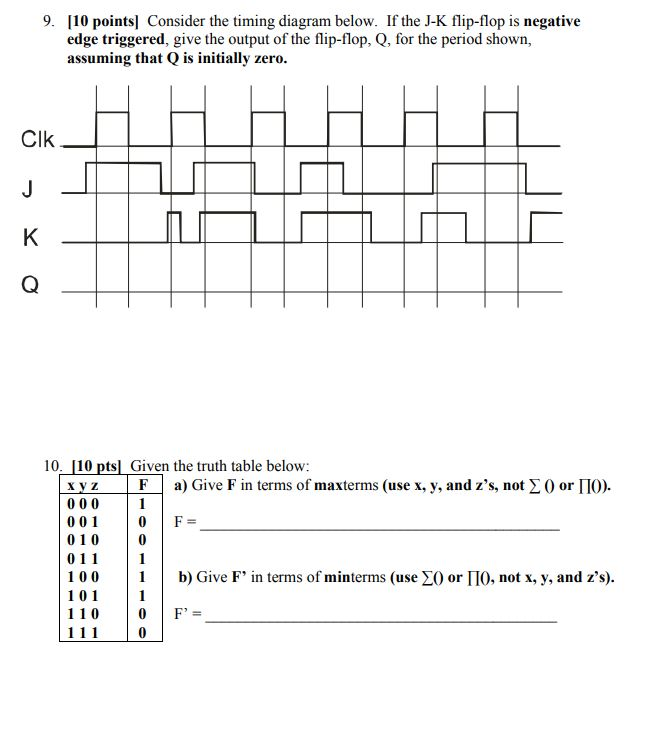
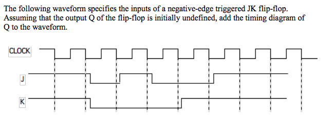
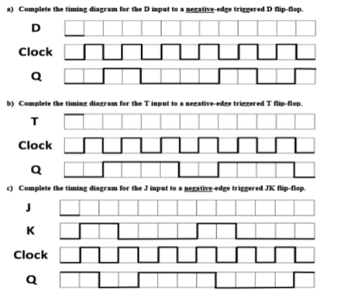
2. Fill in the timing diagram for a falling-edge-triggered J-K flip-flop. (a) Assume Q begins at 0. (b) Assume Q begins at 1, but Clock, J, and K are the same. 3. (a) Find the input for a rising-edge-triggered D flip-flop that would produce the output Q as shown. Fill in the timing diagram. (b) Repeat for a rising-edge-triggered T flip-flop.

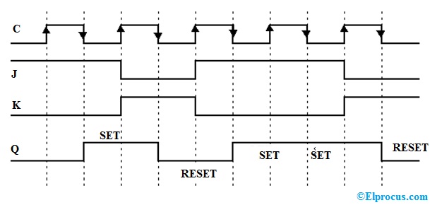
JK flip-flop is a sequential bi-state single-bit memory device named after its as Table II timing diagram for positive edge-triggered jk flip. From the timing diagram it is clear that the output Q changes only at the positive edgeAt each positive edge the output Q becomes equal to the input D at that instant and this value of Q is held untill ...

Each D flip-flop is negative edge-triggered and has a propagation delay for 10 nanoseconds (ns). Develop a timing diagram showing the Q output of each flip-flop, and determine the total propagation delay time from the triggering edge of a clock pulse until a corresponding change can occur in the state of Q3.
A T flip flop is known as a toggle flip flop because of its toggling operation. It is a modified form of the JK flip flop. A T flip flop is constructed by connecting J and K inputs, creating a single input called T. Hence why a T flip flop is also known as a single input JK flip flop. The defining characteristic of T flip flop is that it can ...
The logic circuit diagram of the ripple decade counter can be drawn using negative-edge triggered JK flip-flop as: At the trailing edge of the 10th pulse, the counter temporarily becomes 1010 state, but immediately resets to 0000, since the output of the NAND gate is connected to reset or CLR inputs of flip-flops counter enter into 0000 state ...
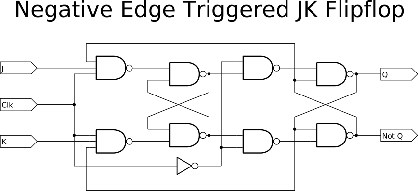
While this implementation of the J-K flip-flop with four NAND gates works in principle there are problems that arise with the timing. JK flip flop is a refined improved version of SR Flip Flop. In the 3-bit ripple counter three flip-flops are used in the circuit. JK Flip-flop Circuit diagram and Explanation. This flip-flop is a negative edge ...
The page you are looking for might have been removed, had its name changed, or is temporarily unavailable · Please check the address bar to make sure the link is typed correctly, use the links below to locate the information you want, or search the site for another destination
A flip-flop is an electronic circuit that can store single-bit binary data either logic 0 or logic 1. Basically, a flip flop is a Bistable multivibrator that changes its output depending on the input. Flip Flops are of two types edge triggered and level triggered. State of an Edge triggered flip flop changes during the positive or negative edge ...

It can also be used for counting of pulses, and for synchronizing variably-timed input signals to some reference timing signal. Flip-flops can be either level-triggered (asynchronous, transparent or opaque) or edge-triggered (synchronous, or clocked). The term flip-flop has historically referred ...

In the T flip - flop, a pulse train of narrow triggers are provided as input (T) which will cause the change in output state of flip - flop. So, these flip - flops are also called Toggle flip - flops. The circuit diagram of a T flip - flop constructed from SR latch is shown below.
April 20, 2021 - Electronics Tutorial about the D-type Flip Flop also known as the Delay Flip flop, Data Latch or D-type Transparent Latch used in Sequential Circuits
June 11, 2019 - A Counter is a device, which stores ... of times a particular event has occurred, often in relationship to a CLOCK Signal. In electronics, counters can be implemented quite easily using memory devices such as Flip-flops. J-K Flip-flop is one of the most commonly used Flip-flops. Table 1 is the Truth-Table of a Negative-Edge-Triggered J-K ...
July 3, 2006 - The JK flip-flop is usually negative edge triggered. The truth table for a negatively triggered JK flip-flop: The timing diagram for the negatively triggered JK flip-flop:


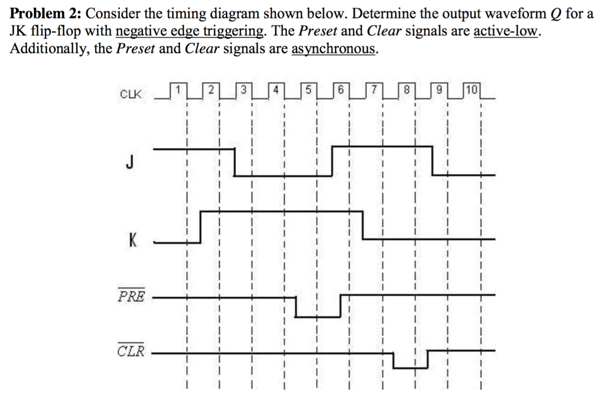


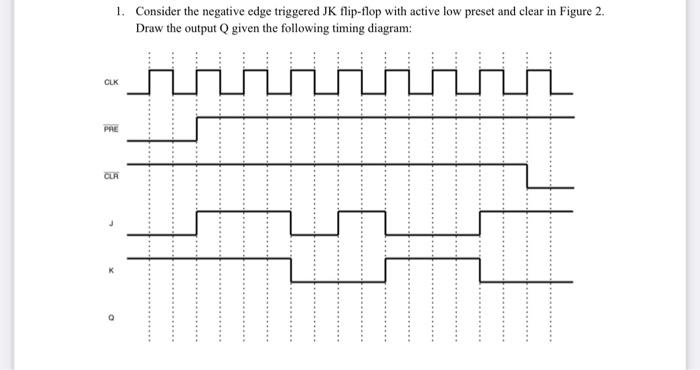

0 Response to "39 negative edge triggered jk flip flop timing diagram"
Post a Comment